























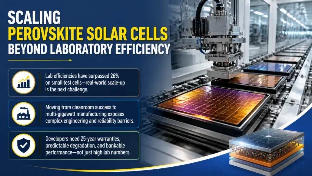
Laboratory records for perovskite solar cells have repeatedly surpassed 26 percent on sub-square-centimeter test substrates, yet translating these synthetic metal-halide absorbers into multi-gigawatt factory output presents engineering barriers that cleanroom environments rarely expose. Solar developers and utility procurement teams evaluate photovoltaic modules on twenty-five-year operational warranties, predictable degradation curves, and dependable bankability metrics.
Metal-halide perovskite solar cells possess direct bandgaps and remarkable light absorption coefficients that allow layers less than one micron thick to harvest sunlight effectively. However, moving from microscopic coin-sized cells to full-size utility modules creates a severe efficiency deficit, often termed the lab-to-fab scaling gap, where resistive power losses and chemical inconsistencies accumulate across large glass sheets.
Industrial commercialization requires mastering the deposition of uniform, pinhole-free crystalline thin films across square meters of moving substrate. Simultaneously, plant operators must protect these volatile organic-inorganic crystal lattices from atmospheric water vapor, ultraviolet radiation, and thermal cycling. Rather than chasing fractional percentage gains in academic research facilities, leading module makers and equipment suppliers now concentrate their capital expenditures on defect passivation, high-speed fluid coating, atomic layer barrier deposition, and automated quality verification.
Overcoming the Industrial Deposition Deficit
Producing thin-film absorbers at industrial throughput requires an abrupt departure from laboratory spin-coating, a technique that wastes more than ninety percent of precursor chemicals and cannot scale across standard solar glass plates. Industrial fabs rely on roll-to-roll or sheet-to-sheet slot-die coating, chemical vapor deposition, and automated blade printing to achieve rapid crystallization. Each coating approach must govern solvent evaporation rates, wet-film drying dynamics, and crystal nucleation kinetics across areas exceeding two square meters without creating microscopic structural defects.

A persistent operational hurdle is the non-uniform formation of intermediate solvated phases. As liquid precursor ink is deposited onto moving glass sheets, drying variations across the surface create microscopic thickness differentials and pinholes. These physical irregularities trigger localized shunts and accelerate non-radiative recombination, pulling module-level conversion efficiency down by three to five percentage points relative to small cells.
- Slot-die coating systems maintain chemical delivery tolerances within three nanometers across broad substrate widths to prevent phase segregation during drying.
- Vacuum-assisted drying chambers replace traditional heated nitrogen knives to achieve rapid, uniform solvent extraction across wide-format glass carriers.
- In-line photoluminescence imaging tools detect microscopic pinholes and crystallographic variations at line speeds exceeding thirty meters per minute.
- Laser patterning protocols establish monolithic P1, P2, and P3 interconnect scribes with dead zones narrower than one hundred and fifty micrometers to maximize active aperture area.
Minimizing interconnect dead zones remains essential for commercial viability. Unlike crystalline silicon modules that use soldered metal ribbons to link individual wafers, thin-film perovskite solar cells rely on monolithic laser scribing to segment the continuous semiconductor coating into series-connected cells. Scribing precision governs module resistance. Any thermal damage or burr formation around the laser kerf compromises insulation resistance, reducing the overall fill factor.
Managing Phase Instability and Chemical Durability
The chemical elegance that gives perovskite crystal structures their optoelectronic qualities also makes them vulnerable to external environmental stressors. Standard methylammonium lead iodide formulations suffer from low thermal decomposition thresholds, breaking down into volatile gaseous byproducts at temperatures routinely encountered under midday desert sunlight. To resolve this vulnerability, industrial material formulators replace volatile organic components with mixed-cation, mixed-halide recipes combining formamidinium, cesium, and rubidium.
Compositional engineering has pushed thermal degradation thresholds well above eighty-five degrees Celsius, meeting standard baseline qualification criteria. Moisture sensitivity nevertheless demands advanced packaging strategies. Water molecules rapidly penetrate the perovskite lattice, initiating irreversible hydrolysis that converts photoactive black perovskite phases into transparent non-absorbing yellow phases. Preventing moisture ingress requires hermetic encapsulation far superior to the ethylene-vinyl acetate sheets used in conventional silicon panel assembly.
Industrial cell producers deploy polyolefin elastomers combined with polyisobutylene edge seals that offer water vapor transmission rates below ten to the negative four grams per square meter per day. In addition, developers apply sub-nanometer aluminium oxide barrier coatings directly onto active device stacks via spatial atomic layer deposition. These impermeable moisture barriers prevent water molecules from reaching the delicate interfaces while stopping volatile halide species from migrating toward external metallic contacts.
Global Manufacturing Initiatives and Pilot Programs
Established module producers and advanced materials enterprises are investing heavily in pilot lines and demonstration manufacturing centers to de-risk high-volume tooling before commissioning multi-gigawatt factories. These programs focus on solvent recovery, environmental safety, toxic lead containment, and automated yield management under industrial cycle times.
- Hanwha Qcells completed a substantial upgrade to its pilot manufacturing operations in 2025, validating high-volume defect passivation chemistries that preserve charge carrier lifetimes across commercial-scale glass formats.
- LONGi Green Energy Technology advanced automated in-line optical inspection and spatial deposition tooling within its research centers, targeting film thickness uniformity variations of less than two percent on large substrates.
- First Solar expanded its dedicated thin-film development initiatives, deploying high-throughput vacuum deposition infrastructure to evaluate inorganic barrier layers and high-durability contact stacks.
- Trina Solar conducted extensive trials at its State Key Laboratory of Photovoltaic Science and Technology, testing monolithic laser scribing parameters on perovskite sub-modules to achieve aperture ratios above ninety-one percent.
- Canadian Solar progressed engineering evaluations on cross-linked polymer encapsulants and low-temperature edge sealing methods designed specifically to prevent chemical leakage and moisture penetration in field operations.
These manufacturing initiatives demonstrate that the technical focus of major manufacturers has transitioned from theoretical physics to process repeatability. Production yields on pilot lines have climbed from forty percent to over eighty percent within two years, demonstrating clear progression toward commercial viability.
Economics, Capital Costs, and Deployment Models
Capital expenditure per watt of manufacturing capacity represents a compelling commercial driver for scaling perovskite solar cells. Conventional crystalline silicon manufacturing demands energy-intensive metallurgical refining, polysilicon chemical purification, high-temperature ingot growth at fourteen hundred degrees Celsius, diamond wire wafer slicing, and multi-step cell diffusion furnaces. In contrast, solution-processed perovskite deposition operates at process temperatures below one hundred and fifty degrees Celsius, slashing manufacturing energy consumption and reducing fab tooling investments.
Lower thermal budgets translate into compressed capital payback timelines. A greenfield perovskite solar cell manufacturing facility requires less heavy machinery and floor space than an integrated polysilicon-to-module complex. However, until balance-of-system durability and thirty-year field reliability are proved in utility installations, project financiers will continue applying risk premiums to pure perovskite arrays.
Large utility developers evaluate total cost of electricity based on real-world degradation rates. A solar module that degrades at two percent annually yields substantially lower lifetime returns than a premium silicon module degrading at zero point four percent, even if initial capital acquisition costs are lower. Consequently, the commercial adoption curve depends heavily on whether encapsulation systems can maintain annual power loss rates under zero point eight percent during twenty-year outdoor exposure tests.

Industrial roadmaps indicate that standalone single-junction perovskite solar cell modules will initially target building-integrated photovoltaics, mobile power systems, and specialty consumer infrastructure where lightweight form factors and high power-to-weight ratios command premium pricing. At the same time, Tier 1 solar executives recognize that combining thin-film perovskite layers with proven crystalline silicon wafers creates the fastest route to capturing mainstream utility market share, establishing tandem solar cells as the dominant strategic pathway for gigawatt-scale production lines across the global PV sector.
Accelerated Lifetime Testing and Environmental Qualification
Before institutional investors and independent engineers approve non-recourse debt financing for utility projects deploying new cell chemistries, modules must withstand rigorous accelerated stress testing. Traditional certification protocols under international standard IEC 61215 were engineered around crystalline silicon failure modes, including solder joint fatigue, cell cracking, and ethylene-vinyl acetate browning. Thin-film perovskites display unique degradation phenomena, including ion migration, phase separation under electrical bias, and light-induced metastable defects.
Leading testing laboratories, including the Fraunhofer Institute for Solar Energy Systems ISE, implement enhanced stress protocols that combine damp-heat exposure, continuous maximum power point tracking under illumination, and rapid thermal cycling. Standard tests subject test specimens to one thousand hours of eighty-five degrees Celsius temperature and eighty-five percent relative humidity. To prove bankability, Tier 1 manufacturers subject prototype modules to extended tests running three thousand hours or more while monitoring chemical stability.
Recent multi-stress trials demonstrate that modules utilizing mixed-cation formulations and multi-layer inorganic encapsulation can maintain ninety-five percent of initial power output after fifteen hundred hours of accelerated testing. PowerGen Advancement notes that progress in chemical passivation, combined with hermetic edge sealing, confirms that industrial perovskite packaging can mitigate the operational vulnerabilities that historically confined these absorbers to laboratory benches.
References
- “Operational Stability and Degradation Pathways of Metal Halide Perovskites” – Fraunhofer Institute for Solar Energy Systems ISE
- “Accelerated Environmental Stress Testing for Next-Generation Photovoltaic Modules” – Hanwha Qcells
- “Large-Scale Thin-Film Deposition Tooling and Uniformity Controls” – LONGi Green Energy Technology
- “Advanced Thin-Film Photovoltaic Research and Vacuum Coating Platforms” – First Solar
- “Monolithic Interconnection and Laser Scribing Optimization for Perovskite Modules” – Trina Solar
- “Advanced Packaging Materials and Moisture Barrier Formulations for Photovoltaics” – Canadian Solar
- “Global Photovoltaic Technology Transition and Levelized Cost Projections” – International Renewable Energy Agency