
























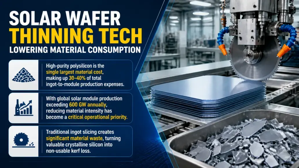
High-purity polysilicon represents the single largest material cost component in photovoltaic manufacturing, accounting for thirty to forty percent of total ingot-to-module production expenses. As the global solar industry scales beyond six hundred gigawatts of annual module production, reducing material intensity has become an operational imperative for upstream manufacturers. Ingot slicing has historically generated substantial material waste, converting expensive crystalline silicon into non-recoverable sawdust during cutting. Today, solar wafer thinning technology is fundamentally transforming ingot processing, enabling wafer manufacturers to slice silicon ingots into ultra-thin substrates while shrinking diamond wire diameters to protect corporate operating margins.
PowerGen Advancement observes that the transition toward solar wafer thinning represents a delicate engineering balance between material conservation and mechanical yield. Over the past decade, standard silicon wafer thickness declined steadily from two hundred micrometers to approximately one hundred and fifty micrometers for mainstream p-type passivated emitter cells. With the sector-wide shift to n-type architectures such as tunnel oxide passivated contacts and silicon heterojunctions, manufacturers are aggressively pushing thicknesses below one hundred and thirty micrometers, with pilot lines validating one hundred and ten micrometer and ninety micrometer substrates.
Diamond Wire Slicing Mechanics and Kerf Loss Reduction
Wafering operations rely on multi-wire saws that move thousands of meters of continuous wire across cylindrical or rectangular silicon ingots at linear speeds exceeding two thousand meters per minute. The cutting mechanism relies on electroplated diamond wire, where micron-sized synthetic diamond abrasives are bonded to a high-tensile core wire via nickel electroplating. Reducing the thickness of the final wafer yields more wafers per meter of ingot, but real material savings require concurrently minimizing kerf loss.
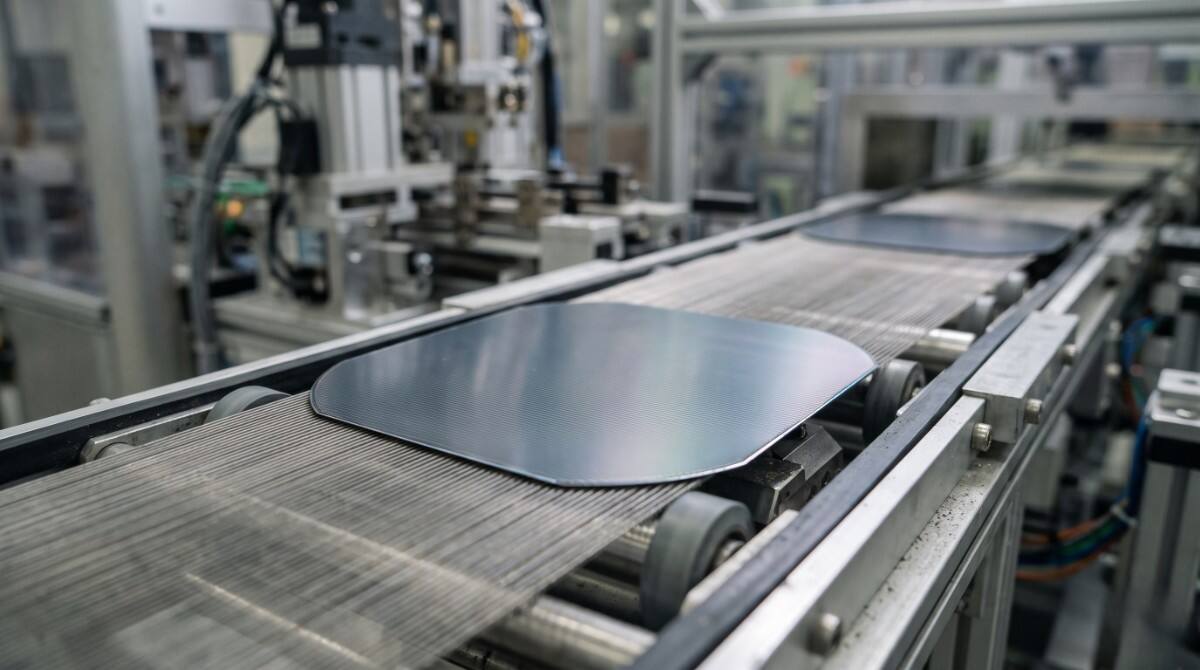
Kerf loss represents the thickness of silicon destroyed and washed away as slurry during the sawing cut. If a sawing wire is forty micrometers thick, it removes roughly forty-five to fifty micrometers of silicon kerf for every cut. If kerf loss equals or exceeds the thickness of the sliced wafer, the economic benefit of thin slicing diminishes rapidly.
- High-tensile tungsten core wires replace traditional carbon steel, allowing wire diameters to decrease from forty micrometers to below thirty-two micrometers without increasing wire break frequency.
- Precision wire tension controllers maintain dynamic tension fluctuations below zero point five Newtons across multi-wire webs carrying hundreds of kilometers of running wire.
- Specialized water-based cutting coolants optimize hydrodynamic lubrication, rapidly extracting cutting heat while suppressing subsurface microcrack formation.
- Automated ingot feed systems match lowering speeds to diamond grit wear rates, maintaining uniform cutting force across large-format rectangular ingots.
Tungsten wire has proven pivotal in enabling thin-wafer production. Tungsten possesses higher ultimate tensile strength and lower elongation under stress compared to high-carbon steel wire. This mechanical rigidity enables machine operators to run thinner wires at higher tension without risking catastrophic web breaks that destroy entire silicon ingots during mid-cut processing.
Cell Processing Lines and Mechanical Handling Dynamics
While wafer manufacturers can slice ingots into wafers thinner than one hundred and twenty micrometers with high yield, downstream cell fabrication lines face formidable processing obstacles. Standard cell processing involves dozens of chemical wet benches, automated belt furnaces, vacuum deposition chambers, and high-speed robotic transfer arms. As wafers become thinner, their mechanical flexibility increases, making them prone to mechanical deformation, microcracking, and chipping.
Thermal warpage represents a severe bottleneck in high-temperature cell lines. Tunnel oxide passivated contact cell manufacturing requires furnace diffusions and annealing steps operating between seven hundred and fifty and eight hundred and fifty degrees Celsius. Uneven thermal gradients across an ultra-thin wafer during rapid heating and cooling cycles induce thermal stresses that cause wafer bowing. If a wafer bows by more than two millimeters, screen-printing metallization fingers become misaligned, and automated vacuum chucks lose suction grip, triggering line stoppages.
In contrast, silicon heterojunction manufacturing operates entirely below two hundred and twenty degrees Celsius. The absence of high-temperature furnace processing makes heterojunction cell lines uniquely compatible with ultra-thin wafers. Heterojunction pilot lines routinely process wafers measuring one hundred and ten micrometers with cell breakage rates below zero point five percent, providing a clear manufacturing advantage as wafer thinning accelerates.
To prevent mechanical damage on thin substrates, automation suppliers deploy non-contact Bernoulli transfer grippers and acoustic levitation chucks. These tools utilize compressed gas or acoustic waves to lift and transport fragile wafers without physical surface contact, preserving wafer edge integrity through automated cell sorting.
Ingot Producers Driving Industrial Thin-Wafer Scaling
Global ingot and wafer producers with immense manufacturing capacity are establishing the technical standards and operational baselines for high-speed thin-wafer slicing. These corporations integrate crystal pulling physics, wire sawing dynamics, and automated defect metrology to deliver uniform thin wafers at multi-gigawatt scale.
- TCL Zhonghuan Renewable Energy Technology Co., Ltd. commercialized ultra-thin large-format wafers across its two-hundred-and-ten millimeter platforms, driving volume production down to one hundred and thirty and one hundred and ten micrometers while applying sub-thirty-four micrometer diamond wires.
- LONGi Green Energy Technology refined diamond wire slicing kinematics and thermal field controls during ingot pulling, establishing standardized thin-wafer specifications across M10 formats to minimize wafer breakage across cell partner lines.
- Tongwei Co., Ltd. advanced integrated ingot-to-cell evaluations, validating one hundred and twenty micrometer n-type wafers across automated high-efficiency cell lines to reduce polysilicon consumption per watt.
- JinkoSolar implemented advanced high-speed optical inspection and resonance testing tools across its manufacturing bases, qualifying large-scale commercial cell production using thin n-type substrates.
- Canadian Solar progressed thin-wafer qualification initiatives within its integrated manufacturing facilities, evaluating kerf-loss reduction tools and the mechanical durability of finished modules built with thin silicon cells.
These enterprise programs confirm that solar wafer thinning is an industry-wide commercial movement rather than an isolated experiment. Process standardization has enabled cell manufacturers to adapt existing automated lines to thinner substrates without incurring prohibitive capital tooling replacement costs.
Polysilicon Consumption Economics and Embodied Carbon
The primary commercial incentive behind solar wafer thinning technology is the reduction of silicon consumption per watt of peak module capacity. In legacy manufacturing setups using one hundred and seventy micrometer wafers and thick diamond wires, producers consumed between two point six and two point eight grams of polysilicon per watt. By reducing wafer thickness to one hundred and thirty micrometers and cutting kerf loss, polysilicon consumption drops to two point zero grams per watt, with advanced lines approaching one point seven grams per watt.
For a gigawatt-scale module manufacturer producing ten gigawatts annually, reducing polysilicon consumption by zero point five grams per watt saves five thousand metric tons of high-purity polysilicon each year. This translates directly into tens of millions of dollars in recurring annual cash savings.
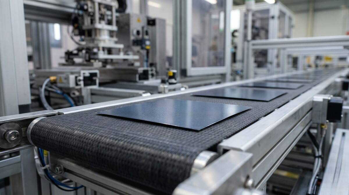
Beyond direct cost reduction, solar wafer thinning delivers profound environmental benefits by lowering module embodied carbon. Polysilicon synthesis through the Siemens process or fluidized bed reactors requires intense electrical energy to vaporize and refine chlorosilane gases. Because the polysilicon manufacturing phase accounts for up to sixty percent of a finished solar module carbon footprint, reducing the mass of silicon per watt significantly reduces product lifecycle emissions. This carbon reduction provides a crucial competitive advantage in European, North American, and Asian public procurement auctions where low-carbon manufacturing thresholds determine tender awards.
While aggressive wafer slicing drives silicon consumption to its physical handling boundary, researchers and equipment makers recognize that the ultimate limit of material reduction lies in eliminating silicon bulk altogether, directing long-term capital investments back toward thin-film absorbers highlighted in scaling perovskite solar cells.
Roadmaps and the One-Hundred-Micrometer Boundary
Industry roadmaps, including the International Technology Roadmap for Photovoltaic published by the German engineering federation VDMA, project that wafer thicknesses for n-type cells will converge toward one hundred and twenty micrometers across mainstream production lines over the next three years. Pushing beyond the one-hundred-micrometer boundary, however, introduces thermodynamic and optical limits.
Crystalline silicon is an indirect bandgap semiconductor with relatively weak light absorption in the near-infrared spectrum. When wafer thickness drops below one hundred micrometers, long-wavelength photons begin passing straight through the silicon absorber without generating electron-hole pairs, reducing short-circuit current density. Compensating for this optical loss requires advanced light-trapping textures and high-reflectivity rear dielectric mirrors.
Equipment manufacturers and wafer producers continue refining tungsten wire drawing, slurry chemistry, and automated cassette handling to ensure that mechanical yields remain above ninety-eight percent. PowerGen Advancement notes that as these engineering systems mature, thin-wafer slicing will remain one of the most effective levers for lowering solar manufacturing costs and expanding global photovoltaic production.
References
- “Ultra-Thin Large-Format Silicon Wafer Slicing and Industrial Yields” – TCL Zhonghuan Renewable Energy Technology Co., Ltd.
- “Diamond Wire Sawing Technology and Kerf Loss Reduction in Ingot Processing” – LONGi Green Energy Technology
- “Integrated N-Type Photovoltaic Cell Manufacturing and Polysilicon Intensity” – Tongwei Co., Ltd.
- “High-Throughput Quality Metrology for Thin-Wafer Solar Cell Lines” – JinkoSolar Holding Co.
- “Mechanical Durability and Environmental Stress Testing on Thin-Wafer Modules” – Canadian Solar Inc.
- “Silicon Material Conservation and Photovoltaic Manufacturing Economics” – Fraunhofer Institute for Solar Energy Systems ISE
- “International Technology Roadmap for Photovoltaic (ITRPV) Fifteenth Edition” – VDMA German Engineering Federation