
























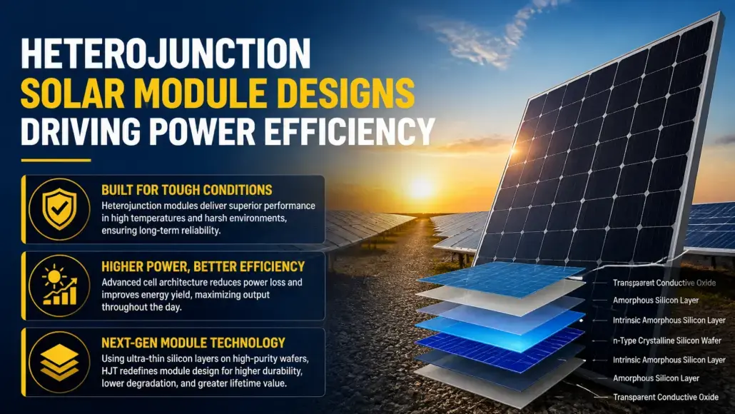
Utility-scale solar developers face tightening project margins and increasingly severe operational climates, forcing engineering teams to prioritize module durability and performance under elevated temperatures. While passivated emitter and rear cell technology anchored the previous decade of solar expansion, silicon heterojunction technology has emerged as a high-performance standard that fundamentally redefines module design. By depositing nanometer-thin amorphous silicon films onto high-purity crystalline silicon base wafers, manufacturers achieve superior surface passivation, pushing open-circuit voltages beyond seven hundred and fifty millivolts and unlocking unprecedented energy conversion yields.
The architectural distinction of heterojunction devices lies in their symmetrical, low-temperature construction. Conventional diffused-junction solar cells require multiple high-temperature thermal steps exceeding eight hundred degrees Celsius to form p-n junctions and fire metallic contact pastes. In contrast, heterojunction solar cells are fabricated entirely below two hundred and twenty degrees Celsius, preserving bulk silicon wafer quality while dramatically reducing manufacturing thermal budgets. This design enables higher energy yield per watt installed, transforming utility system economics in regions characterized by high solar irradiance and extreme ambient temperatures.
Physics and Design of Amorphous Silicon Passivation
The foundation of heterojunction solar module efficiency rests on suppressing surface carrier recombination. In a standard crystalline silicon wafer, abrupt termination of the crystal lattice at the wafer surface leaves dangling atomic bonds that act as potent recombination centers, trapping photogenerated charge carriers before they can be collected as electrical current. Heterojunction architecture neutralizes this vulnerability by depositing ultra-thin intrinsic amorphous silicon passivating layers onto both sides of an n-type crystalline silicon wafer.

Plasma-enhanced chemical vapor deposition chambers introduce silane and hydrogen gas mixtures at strictly regulated dilution ratios to grow these amorphous films. Hydrogen radicals passivate dangling bonds at the crystalline interface, extending charge carrier lifetimes to several milliseconds. Immediately following the intrinsic layer, thin doped amorphous silicon layers are applied to create carrier-selective contacts: a p-type doped layer on one side to extract holes and an n-type doped layer on the opposing side to collect electrons. Because amorphous silicon has a wider bandgap than crystalline silicon, this arrangement creates an internal band bending that repels minority carriers, driving surface recombination velocities to near-zero levels.
- Intrinsic amorphous silicon layers measuring between three and five nanometers in thickness passivate silicon surface defects without impeding carrier transport.
- Plasma-enhanced chemical vapor deposition systems balance silane dilution ratios to achieve optimal silicon-hydrogen bonding configurations without micro-crystallite formation.
- Wide-bandgap doped amorphous silicon contact layers establish robust internal electric fields, generating open-circuit voltages exceeding seven hundred and fifty millivolts.
- Magnetron sputtering systems deposit transparent conductive oxide layers, such as indium tin oxide, to provide lateral electrical conductivity and optical antireflection.
- Low-temperature metallization pastes cure below two hundred degrees Celsius, protecting the delicate amorphous silicon and hydrogen bonding network from thermal breakdown.
Transparent conductive oxide layers play a pivotal role in device operation. Because amorphous silicon films exhibit high electrical resistivity, sputtered conductive oxides are essential to transport photogenerated charges laterally toward the screen-printed metallic fingers while optimizing optical transmission across the visible and infrared spectrum.
Thermal Coefficients and Bifacial Performance Advantages
Operating temperature is one of the most significant external factors undermining field performance in photovoltaic plants. Standard p-type PERC and even newer tunnel oxide passivated contact modules suffer power output drops between zero point three zero and zero point three eight percent for every degree Celsius the cell temperature rises above the standard testing baseline of twenty-five degrees Celsius. In desert installations where operating cell temperatures regularly reach sixty-five degrees Celsius, these thermal losses degrade project revenue.
Silicon heterojunction solar modules deliver a temperature coefficient between minus zero point two four and minus zero point two six percent per degree Celsius. This thermal stability translates into an immediate three to five percent generation advantage during peak midday summer hours, precisely when electricity market prices and grid demand peak.
Bifaciality represents another core operational advantage stemming directly from symmetrical cell architecture. Because the front and rear faces of a heterojunction solar cell are fabricated with identical thin-film layers and transparent conductive oxides, the rear side achieves a bifaciality factor between eighty-five and ninety-five percent. In comparison, competing architectures achieve rear-side generation factors between seventy and eighty percent. When mounted on single-axis trackers over high-albedo soils such as light gravel, sand, or snow, heterojunction solar modules capture substantial reflected and diffuse irradiation, delivering compounding kilowatt-hour gains across the asset lifecycle. Single-axis tracker algorithms with bifacial backtracking adjust tracking angles in real time to capture optimal diffuse ground reflection, unlocking higher financial returns for power asset owners.
Tier 1 Deployments and Manufacturing Expansions
Commercial adoption of heterojunction solar technology has accelerated as global manufacturers commission multi-gigawatt production lines and demonstrate successful utility-scale deployments across competitive power markets. Leading corporations are demonstrating that high-efficiency heterojunction solar modules can be produced at scale while maintaining rigorous defect management and high production yields.
- Risen Energy launched its upgraded Hyper-ion heterojunction solar module series in high-volume production, delivering mass-production power outputs exceeding seven hundred and forty watts with module efficiencies surpassing twenty-three point eight percent.
- Meyer Burger Technology AG advanced industrial production of premium heterojunction modules utilizing patented SmartWire interconnection technology, eliminating standard soldered busbars to minimize mechanical stress on thin wafers.
- Canadian Solar progressed engineering evaluations and pilot manufacturing programs for heterojunction architectures, qualifying specialized low-temperature metallization formulations and highly durable edge-sealing encapsulants.
- Enel S.p.A., through its 3Sun manufacturing subsidiary, expanded clean technology manufacturing infrastructure to scale high-efficiency bifacial heterojunction solar cells and modules for international utility portfolios.
- Tongwei Co., Ltd. operated multi-gigawatt heterojunction pilot and production lines, validating copper electroplating metallization as a high-throughput alternative to conventional screen printing.
These enterprise deployments show that heterojunction solar modules have moved decisively beyond niche residential rooftops into utility-scale procurement pipelines. Independent engineering firms now actively model heterojunction generation curves in bankability evaluations for major energy infrastructure funds.
Overcoming Metallization Bottlenecks and Silver Consumption
The historical impediment to widespread heterojunction manufacturing has been the cost and volume of silver consumed during screen printing. Because heterojunction solar cells cannot withstand the eight-hundred-degree contact-firing temperatures used in conventional solar cells, they require low-temperature silver pastes containing organic binders. These pastes exhibit lower electrical conductivity and slower curing speeds, requiring wider metallization fingers and higher paste volumes that inflate bill-of-materials costs.
To solve this economic challenge, equipment suppliers and cell makers have pioneered silver-coated copper pastes. By encapsulating a copper core within a thin silver shell, manufacturers reduce net silver consumption by thirty to fifty percent without degrading electrical conductivity or long-term contact adhesion.
In parallel, busbarless cell designs have gained broad industrial traction. By eliminating large printed silver busbars and replacing them with dozens of micro-wires embedded into the module lamination film, manufacturers slash metallization laydown while shortening current collection paths. Copper electroplating represents the final frontier in metallization, substituting precious silver entirely with chemical copper deposition. As these metallization breakthroughs enter volume production, the manufacturing cost premium of heterojunction technology continues to narrow.

While heterojunction architectures resolve front and rear surface recombination through amorphous passivating layers, competing manufacturing consortiums are eliminating front shading entirely by moving all electrical polarity contacts to the rear wafer surface, accelerating efforts toward commercializing back-contact solar cells manufacturing across utility and distributed generation markets.
Long-Term Reliability and Bankability Economics
Evaluating thirty-year asset lifecycles requires analyzing intrinsic degradation modes. Traditional solar cells suffer from light-induced degradation and potential-induced degradation, phenomena driven by boron-oxygen defect complexes, sodium ion migration, and electric field stress across module packaging. Heterojunction solar cells utilize n-type base wafers doped with phosphorus, fundamentally eliminating boron-oxygen light degradation.
Furthermore, the transparent conductive oxide layers act as natural equipotential barriers that shield the p-n junction from external electrostatic fields, providing resistance against potential-induced degradation. Commercial heterojunction modules feature comprehensive thirty-year linear power warranties, guaranteeing annual degradation rates below zero point three five percent compared to zero point five zero percent for legacy panels. Independent laboratories subject test modules to extended environmental stress sequences, including three thousand hours of damp-heat testing and six hundred thermal cycles, confirming physical resilience well beyond standard international baselines.
Financial modeling shows that when developers incorporate thirty-year durability, superior temperature coefficients, and high bifacial energy yield into levelized cost of electricity calculations, heterojunction modules provide attractive internal rates of return despite modest initial capital premiums. PowerGen Advancement observes that as supply chain ecosystems for low-temperature pastes, high-purity n-type ingots, and thin-film deposition tools mature, heterojunction solar modules are establishing themselves as a dominant architectural platform for high-performance solar generation.
References
- “High-Efficiency Heterojunction Solar Module Production and Field Reliability” – Risen Energy Co., Ltd.
- “SmartWire Connection Technology for Heterojunction Photovoltaics” – Meyer Burger Technology AG
- “Industrial Scaling of High-Efficiency Bifacial Solar Architectures” – Enel S.p.A.
- “Low-Temperature Metallization and Module Packaging for Heterojunction Cells” – Canadian Solar Inc.
- “Copper Electroplating and Advanced Metallization for Heterojunction Solar Cells” – Tongwei Co., Ltd.
- “Silicon Heterojunction Solar Cells: State of the Art and Industrial Perspectives” – Fraunhofer Institute for Solar Energy Systems ISE
- “Global Renewable Energy Technology Outlook and Photovoltaic Cost Benchmarks” – International Renewable Energy Agency