




















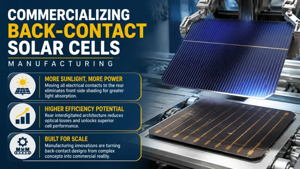
For decades, photovoltaic engineers accepted an unavoidable optical compromise: metallic contact fingers and busbars had to sit on the sun-facing front surface of a solar cell to collect electric current, inevitably shading two to three percent of the active semiconductor surface. Eliminating this optical penalty by moving all positive and negative electrical contacts to the rear wafer surface unlocks superior light absorption. While interdigitated back-contact architectures were historically confined to specialized, high-cost residential rooftops, back-contact solar cell manufacturing is now entering a profound commercial transformation as leading global module makers invest billions to scale back-contact gigafactories for mass-market deployment.
PowerGen Advancement observes that the industrial momentum behind back-contact solar cell designs stems from the convergence of efficiency gains and aesthetic advantages. By freeing the front surface from metal grids, a back-contact solar cell captures every incoming photon, boosting short-circuit current densities to peak theoretical thresholds. Concurrently, the uniform dark appearance of front surfaces appeals strongly to distributed generation buyers. However, the true commercial catalyst is the deployment of high-speed industrial laser patterning, which replaces expensive semiconductor photolithography and allows cell manufacturers to produce intricate rear interdigitated contact patterns at multi-gigawatt line speeds.
Eliminating Optical Shading and Maximizing Front Absorption
The physical advantage of back-contact solar cells begins with total active illumination. In standard front-contact cells, fine screen-printed silver fingers reflect and scatter incoming photons, creating an immediate optical loss that cannot be recovered through antireflection coatings. Back-contact architectures achieve a one-hundred-percent active aperture on the illuminated side, enabling short-circuit current densities to reach forty-two to forty-three milliamperes per square centimeter.
Liberating the front surface also allows engineers to optimize front passivation without balancing electrical contact resistance. In conventional cells, the front emitter must be heavily doped under metal contact lines to ensure low contact resistance, which introduces Auger recombination and parasitic blue-light absorption. With no metal contacts on the front, back-contact solar cells utilize lightly doped, uniform dielectric passivation layers that dramatically reduce surface carrier recombination.
- Complete removal of front metallization eliminates optical shading, maximizing short-circuit current generation across all visible and infrared wavelengths.
- Decoupled front-side passivation minimizes surface recombination velocity while preserving full transmission of high-energy ultraviolet and blue light.
- Interdigitated p-type and n-type doped stripes on the rear surface collect photogenerated holes and electrons through localized electric fields.
- High minority carrier lifetimes exceeding two milliseconds ensure that charge carriers generated near the front surface diffuse through the entire wafer thickness to reach rear contacts.
- Symmetrical stress distributions across the front surface eliminate localized microcrack initiation points commonly caused by front solder ribbons.
Achieving high carrier collection efficiency requires exceptional wafer quality. Photogenerated electrons and holes created near the front surface must travel through the entire bulk thickness of the silicon wafer to reach the collecting junctions on the back side. Consequently, back-contact architectures require high-purity n-type monocrystalline wafers with carrier diffusion lengths significantly greater than wafer thickness.
Laser Patterning and Industrial Process Simplification
The barrier that previously restricted back-contact solar cells to niche markets was fabrication complexity. Early interdigitated back-contact production required multiple photolithographic masking steps, chemical etch-back sequences, and repeated high-temperature furnace diffusions to align alternating p-doped and n-doped stripes on the rear surface. These elaborate cleanroom procedures depressed manufacturing yields and inflated production costs far beyond commercial viability.
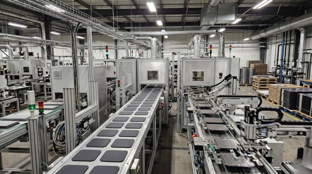
Modern gigawatt-scale production lines have replaced photolithography with precision laser micromachining and self-aligned screen printing. Industrial picosecond and nanosecond laser ablation tools pattern dielectric films and isolation grooves at speeds of thousands of wafers per hour. These laser systems achieve positional alignment accuracy within five micrometers, ensuring reliable isolation between adjacent positive and negative doped regions.
Carefully tuned laser contact opening processes vaporize overlying dielectric layers without inducing micro-cracking or subterranean thermal damage in the underlying silicon crystal. Industrial fabs employ plasma-enhanced chemical vapor deposition and inline low-pressure chemical vapor deposition to deposit micro-thin polysilicon films for passivated contact formation. Laser-assisted local doping introduces localized boron and phosphorus dopant profiles without requiring hazardous chemical masking agents. By consolidating multiple fabrication steps into continuous automated laser and printing sequences, cell makers have driven production yields above ninety-seven percent, approaching the yield benchmarks of mature passivated contact lines.
Mass Production Milestones and Tier 1 Deployments
The global solar sector is witnessing massive capital commitments toward back-contact manufacturing capacity, led by Tier 1 manufacturers that view back-contact architectures as the ultimate platform for crystalline silicon photovoltaics.
- LONGi Green Energy Technology announced a multi-gigawatt strategic transition toward back-contact technology, scaling its Hybrid Passivated Back Contact platform across tens of gigawatts of capacity and launching its Hi-MO 9 utility module featuring commercial efficiencies above twenty-four point four percent.
- Shanghai Aiko Solar Energy Co., Ltd. expanded mass production of its all-back-contact n-type modules, achieving commercial module efficiencies exceeding twenty-four point two percent and delivering over fourteen gigawatts of high-efficiency modules globally.
- Maxeon Solar Technologies progressed manufacturing expansions for its next-generation Maxeon 7 back-contact architecture, leveraging proprietary interdigitated contact tooling to set premium performance benchmarks in distributed generation markets.
- JinkoSolar advanced pilot evaluations and targeted research programs for n-type back-contact architectures, testing advanced passivation layers to assess mass-manufacturing scalability alongside its existing n-type capacity.
- Trina Solar evaluated back-contact cell configurations on large-format two-hundred-and-ten millimeter wafers, investigating rear-side stress distribution and thermal-mechanical stability under industrial lamination processes.
These enterprise deployments demonstrate that back-contact technology is no longer an academic pursuit or a boutique product. High-volume gigafactories in operation today produce millions of back-contact cells monthly, creating intense competitive pressure across the broader photovoltaic supply chain.
Module Assembly Engineering and Interconnection Innovations
Packaging back-contact solar cells into durable modules demands a departure from standard stringing and tab soldering equipment. Conventional modules use copper ribbons that route from the front surface of one cell to the rear surface of the next, creating mechanical bending stress and potential ribbon-drift defects during thermal expansion. In contrast, back-contact solar cells feature all electrical termination pads on the rear surface, enabling planar module interconnection.
Manufacturers deploy conductive backsheet technology or patterned copper-foil backsheets where cells are placed directly onto pre-patterned electrical circuits. Electrically conductive adhesives or low-temperature solder pastes establish metallurgical joints between cell rear contacts and the backsheet circuit in a single automated step. High-speed pick-and-place automation systems utilize optical cameras to register wafer coordinates within twenty micrometers, preventing registration drift before the module enters thermal lamination.
Planar interconnection eliminates cell-to-cell tabbing gaps, allowing module assemblers to achieve high packing density and seamless zero-gap cell spacing. Furthermore, because no soldered ribbons cross over wafer edges, edge-chipping and microcracking induced by mechanical wind or heavy snow loads are substantially mitigated. The resulting module exhibits superior mechanical resilience and resistance against cyclic fatigue during decades of field operation.
As back-contact gigafactories expand production, the reliance on high-purity n-type silicon wafers has heightened commercial sensitivity to raw silicon costs, prompting cell makers to integrate advanced slicing techniques explored in solar wafer thinning.
Market Segmentation and Levelized Cost Economics
Back-contact modules first established commercial dominance in the distributed generation segment, where residential homeowners and commercial building operators place a high value on panel aesthetics and maximum power output per square meter of roof space. The uniform black facade of front-contact-free panels commands pricing premiums in affluent residential markets across Europe, North America, and Australia.
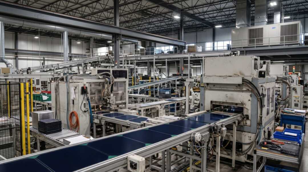
However, PowerGen Advancement notes that the rapid decline in back-contact solar cell manufacturing costs is expanding the technology into utility-scale power projects. Utility developers realize substantial financial gains from higher module efficiency, as twenty-four percent efficient panels generate greater power density and lower balance-of-system costs per installed megawatt. Optimized operating voltages reduce electrical resistance across long string runs, lowering internal cable dissipation losses and optimizing central inverter loading ratios.
Utility-focused back-contact solar cell designs, such as hybrid passivated back-contact modules with rear-side bifacial openings, deliver high energy yield when deployed on single-axis trackers. With annual degradation rates guaranteed below zero point three five percent over thirty-year warranties, back-contact modules are proving that premium cell architectures can compete aggressively on levelized cost of electricity across both distributed rooftops and utility power plants.
References
- “Industrial Hybrid Passivated Back Contact Solar Cell Technology and Module Reliability” – LONGi Green Energy Technology
- “All-Back-Contact High-Efficiency Module Mass Production and Field Data” – Shanghai Aiko Solar Energy Co., Ltd.
- “Interdigitated Back-Contact Cell Architecture and Long-Term Durability” – Maxeon Solar Technologies
- “Advanced N-Type Passivated Contact and Back-Contact Photovoltaic Research” – JinkoSolar Holding Co.
- “Large-Format Wafer Integration for Next-Generation Cell Designs” – Trina Solar Co., Ltd.
- “High-Efficiency Silicon Photovoltaics: Interdigitated Back Contact Perspectives” – Fraunhofer Institute for Solar Energy Systems ISE
- “Photovoltaic Cost and Technology Transition Benchmarks” – International Renewable Energy Agency